Lithography
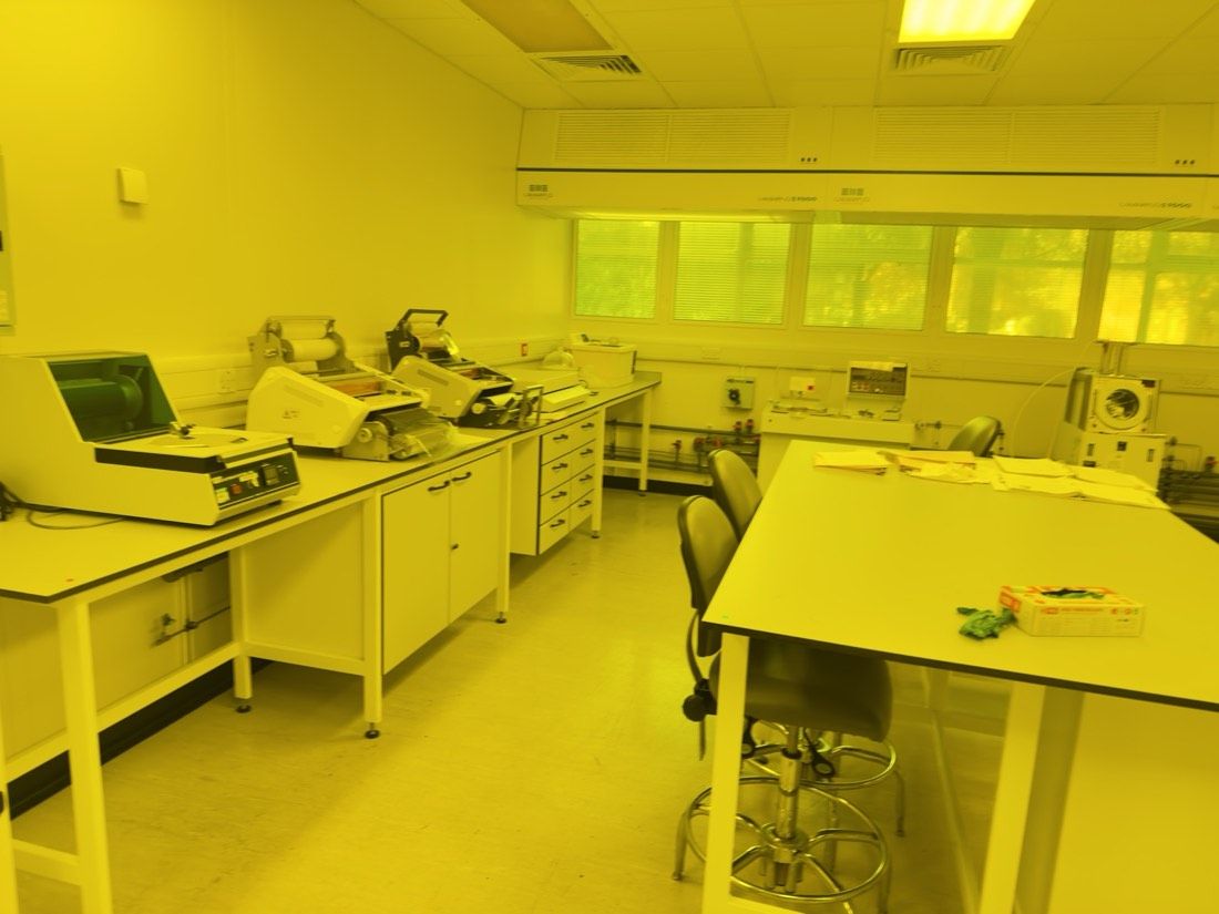
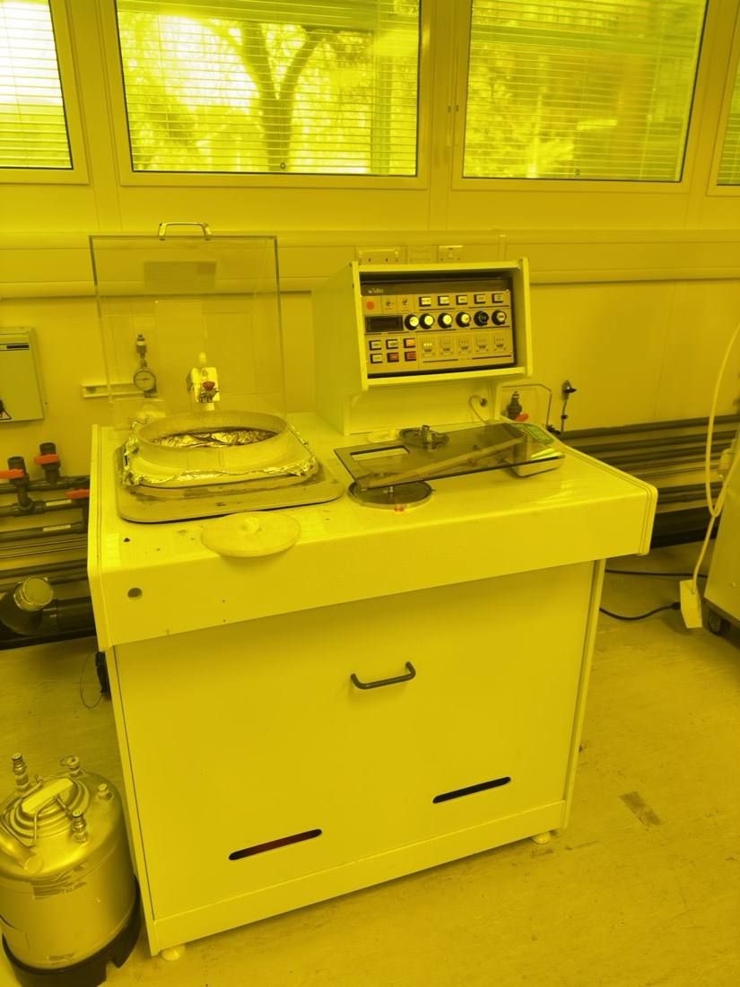
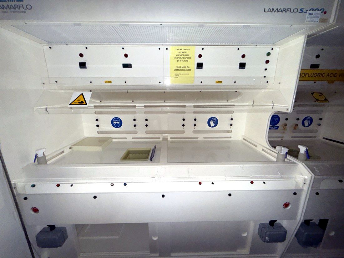
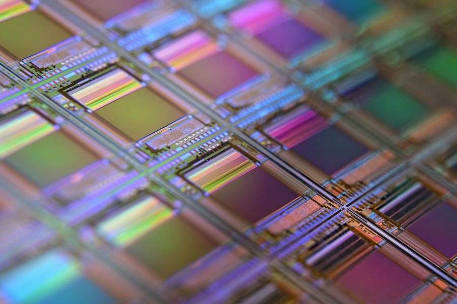
Pattern features onto wafers, from a design file or a mask.
- Maskless direct-write lithography on wafers up to 6 inch, with features down to about 1.1 µm
- Mask-based UV contact lithography on 3-inch wafers
- Patterning for electrodes, masters and device layers