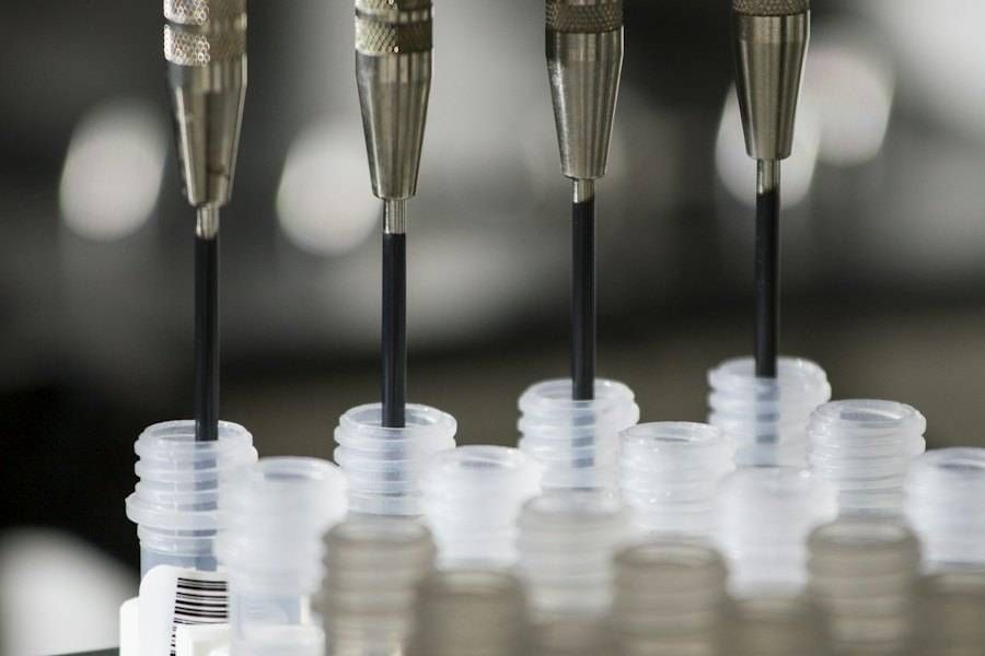
Microfluidics and lab-on-chip
Fluidic chips in silicon, glass and polymers for diagnostics, life sciences and research.
In the toolset: deep silicon etch for channels, oxide insulation, metal electrodes, and PDMS and UV-epoxy handling.
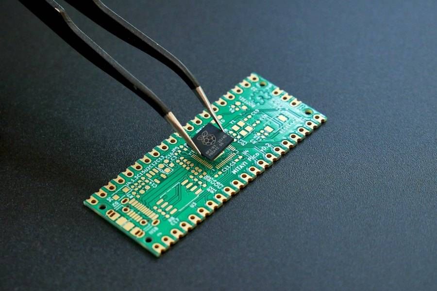
Markets
Ten markets the facility’s toolset is being set up to support. We want to hear from companies and research groups working in these areas, and in others we haven’t listed.
Fluidic chips in silicon, glass and polymers for diagnostics, life sciences and research.
In the toolset: deep silicon etch for channels, oxide insulation, metal electrodes, and PDMS and UV-epoxy handling.
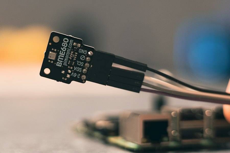
Pressure, inertial, resonant and thermal sensors, from concept to working prototype.
In the toolset: deep silicon etch, furnaces, polysilicon and nitride films. HF vapour release is a planned addition.
Actuators, energy harvesters and acoustic devices.
In the toolset: high-field magnetron sputtering, rapid thermal processing and X-ray diffraction.
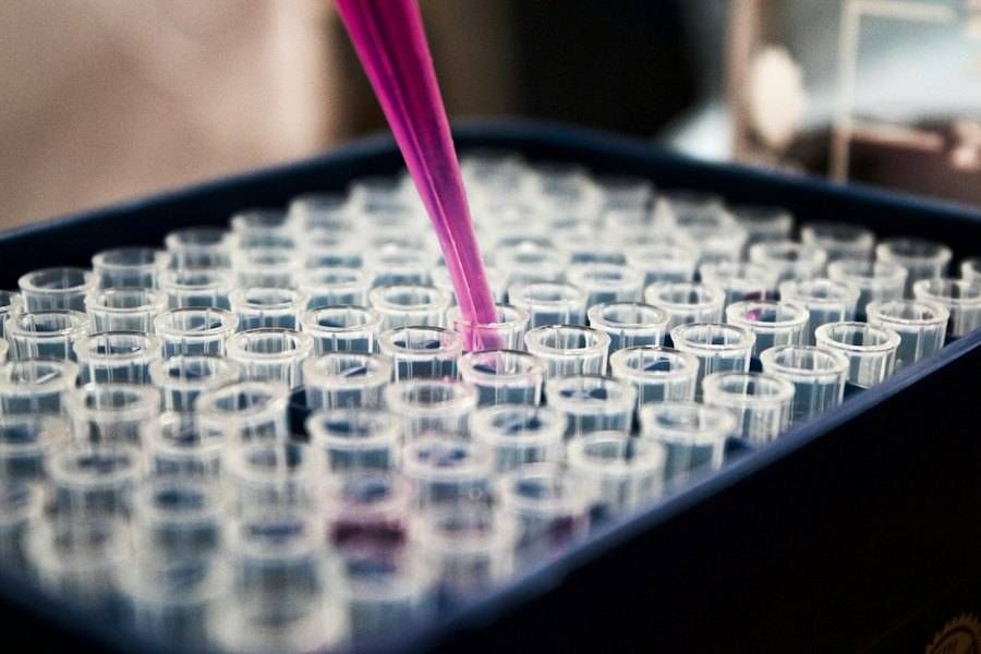
Implant encapsulation and thin-film electrodes for medical and diagnostic devices.
In the toolset: parylene coating, evaporated electrodes, wire bonding and die placement.
Small-batch assembly for start-ups and spin-outs.
In the toolset: dicing, ball and wedge bonding, pull testing and sub-micron die placement.
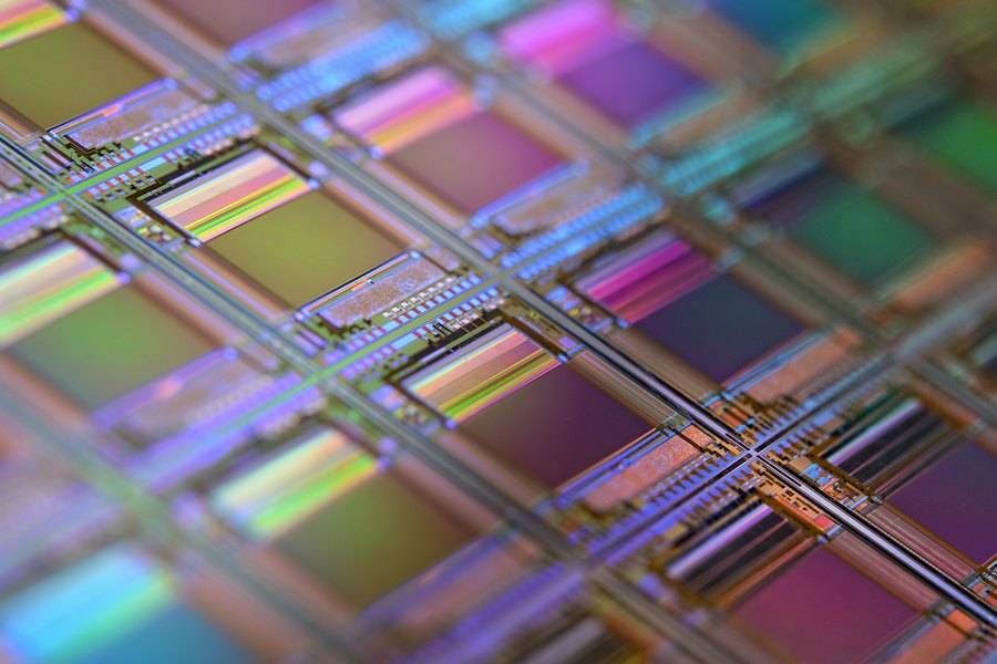
Front-end style research runs before committing to volume production.
In the toolset: furnaces, PE-CVD, deep silicon etch, reactive-ion etch and rapid thermal processing.
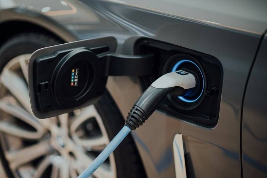
GaN and SiC device work: contacts, mesas and ohmic anneals.
In the toolset: reactive-ion and ICP etch, e-beam contact metals, PE-CVD passivation and rapid thermal anneals.
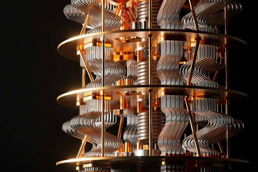
Thin-film circuits and junction work for quantum materials, sensors and devices.
In the toolset: evaporation, sputtering, annealing and reactive-ion etch for film deposition and patterning.
Waveguides, gratings and optical sensors.
In the toolset: PE-CVD oxide and nitride, ICP etch and sputtered films, with SEM and AFM inspection.
Silicon and glass interposers and redistribution layers.
In the toolset: deep silicon etch for through-silicon vias, PE-CVD liners, sputtered barrier and seed layers, lithography and dicing.
If your work is at the micro or nano scale and it isn’t listed here, tell us what you need. It helps us understand what would be most useful to companies.
Headline tools, process areas and the outcomes the facility is being set up to support.